Subscribers are basically listeners of an analysis port. They subscribe to a broadcaster and receive objects whenever an item is broadcasted via the connected analysis port. A uvm_component class does not have an in-built analysis port, while a uvm_subscriber is an extended version with an analysis port named analysis_export.
Class definition
virtual class uvm_subscriber #(type T=int) extends uvm_component;
	typedef uvm_subscriber #(T) this_type;

	uvm_analysis_imp #(T, this_type) analysis_export;

	function new (string name, uvm_component parent);
		super.new (name, parent);
		analysis_export = new ("analysis_imp", this);
	endfunction

	pure virtual function void write (T, t);
endclass
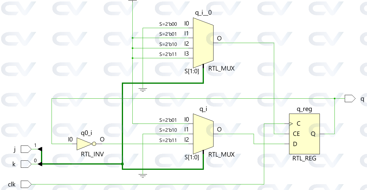
Design
module jk_ff ( input j,
               input k,
               input clk,
               output q);

   reg q;

   always @ (posedge clk)
      case ({j,k})
         2'b00 :  q <= q;
         2'b01 :  q <= 0;
         2'b10 :  q <= 1;
         2'b11 :  q <= ~q;
      endcase
endmodule
Hardware Schematic
Testbench
module tb_jk;
   reg j;
   reg k;
   reg clk;

   always #5 clk = ~clk;

   jk_ff    jk0 ( .j(j),
                  .k(k),
                  .clk(clk),
                  .q(q));

   initial begin
      j <= 0;
      k <= 0;

      #5 j <= 0;
         k <= 1;
      #20 j <= 1;
          k <= 0;
      #20 j <= 1;
          k <= 1;
      #20 $finish;
   end

   initial
      $monitor ("j=%0d k=%0d q=%0d", j, k, q);
endmodule
A D flip-flop is a sequential element that follows the input pin d at the given edge of a clock.
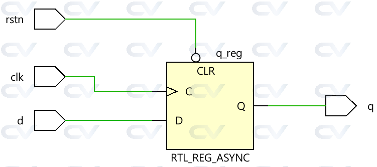
Design #1: With async active-low reset
module dff 	( input d,
              input rstn,
              input clk,
              output reg q);

	always @ (posedge clk or negedge rstn)
       if (!rstn)
          q <= 0;
       else
          q <= d;
endmodule
Hardware Schematic
Testbench
module tb_dff;
	reg clk;
	reg d;
	reg rstn;
	reg [2:0] delay;

    dff  dff0 ( .d(d),
                .rsnt (rstn),
                .clk (clk),
                .q (q));

    // Generate clock
    always #10 clk = ~clk;

    // Testcase
    initial begin
    	clk <= 0;
    	d <= 0;
    	rstn <= 0;

    	#15 d <= 1;
    	#10 rstn <= 1;
    	for (int i = 0; i < 5; i=i+1) begin
    		delay = $random;
    		#(delay) d <= i;
    	end
    end
endmodule
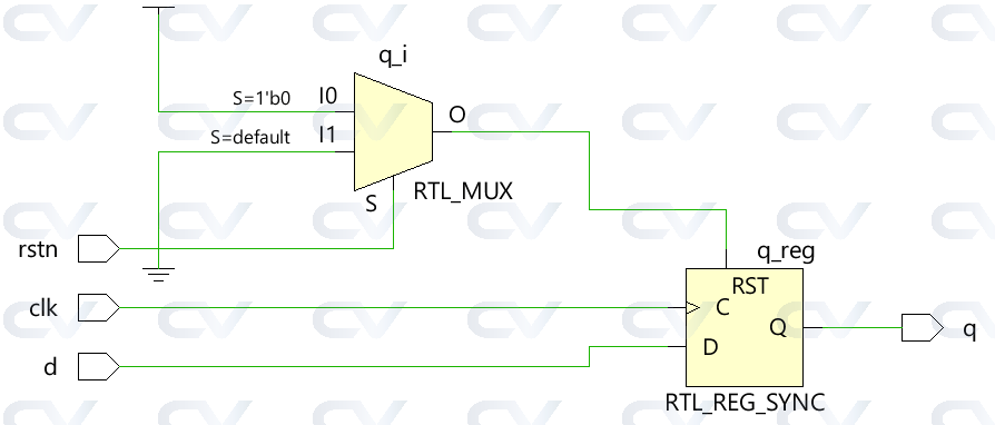
Design #1: With sync active-low reset
module dff 	( input d,
              input rstn,
              input clk,
              output reg q);

	always @ (posedge clk)
       if (!rstn)
          q <= 0;
       else
          q <= d;
endmodule
Hardware Schematic
Testbench
module tb_dff;
	reg clk;
	reg d;
	reg rstn;
	reg [2:0] delay;

    dff  dff0 ( .d(d),
                .rsnt (rstn),
                .clk (clk),
                .q (q));

    // Generate clock
    always #10 clk = ~clk;

    // Testcase
    initial begin
    	clk <= 0;
    	d <= 0;
    	rstn <= 0;

    	#15 d <= 1;
    	#10 rstn <= 1;
    	for (int i = 0; i < 5; i=i+1) begin
    		delay = $random;
    		#(delay) d <= i;
    	end
    end
endmodule
A latch has two inputs : data(D), clock(clk) and one output: data(Q). When the clock is high, D flows through to Q and is transparent, but when the clock is low the latch holds its output Q even if D changes.
A flip-flop on the other hand captures data at its input at the positive or negative edge of a clock and output does not reflect changes in the input until the next clock edge.
Design
In this example, we'll build a latch that has three inputs and one output. The input d stands for data which can be either 0 or 1, rstn stands for active-low reset and en stands for enable which is used to make the input data latch to the output. Reset being active-low simply means that the design element will be reset when this input goes to 0 or in other words, reset is active when its value is low. The value of output q is dictated by the inputs d, en and rstn.
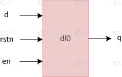
module d_latch (  input d,           // 1-bit input pin for data
                  input en,          // 1-bit input pin for enabling the latch
                  input rstn,        // 1-bit input pin for active-low reset
                  output reg q);     // 1-bit output pin for data output

   // This always block is "always" triggered whenever en/rstn/d changes
   // If reset is asserted then output will be zero
   // Else as long as enable is high, output q follows input d
   always @ (en or rstn or d)
      if (!rstn)
         q <= 0;
      else
         if (en)
            q <= d;
endmodule
In digital electronics, a shift register is a cascade of flip-flops where the output pin q of one flop is connected to the data input pin (d) of the next. Because all flops work on the same clock, the bit array stored in the shift register will shift by one position. For example, if a 5-bit right shift register has an initial value of 10110 and the input to the shift register is tied to 0, then the next pattern will be 01011 and the next 00101.
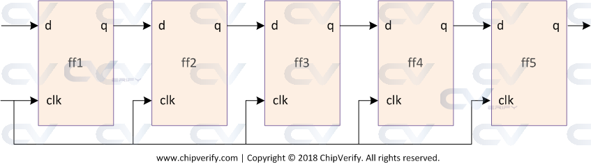
Design
This shift register design has five inputs and one n-bit output and the design is parameterized using parameter MSB to signify width of the shift register. If n is 4, then it becomes a 4-bit shift register. If n is 8, then it becomes an 8-bit shift register.
This shift register has a few key features:
- Can be enabled or disbled by driving en pin of the design
- Can shift to the left as well as right when dir is driven
- If rstn is pulled low, it will reset the shift register and output will become 0
- Input data value of the shift register can be controlled by d pin
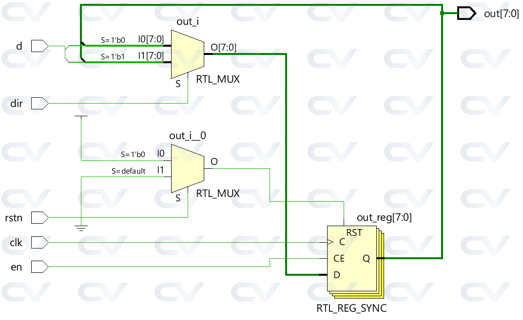
module shift_reg  #(parameter MSB=8) (  input d,                      // Declare input for data to the first flop in the shift register
                                        input clk,                    // Declare input for clock to all flops in the shift register
                                        input en,                     // Declare input for enable to switch the shift register on/off
                                        input dir,                    // Declare input to shift in either left or right direction
                                        input rstn,                   // Declare input to reset the register to a default value
                                        output reg [MSB-1:0] out);    // Declare output to read out the current value of all flops in this register


   // This always block will "always" be triggered on the rising edge of clock
   // Once it enters the block, it will first check to see if reset is 0 and if yes then reset register
   // If no, then check to see if the shift register is enabled
   // If no => maintain previous output. If yes, then shift based on the requested direction
   always @ (posedge clk)
      if (!rstn)
         out <= 0;
      else begin
         if (en)
            case (dir)
               0 :  out <= {out[MSB-2:0], d};
               1 :  out <= {d, out[MSB-1:1]};
            endcase
         else
            out <= out;
      end
endmodule
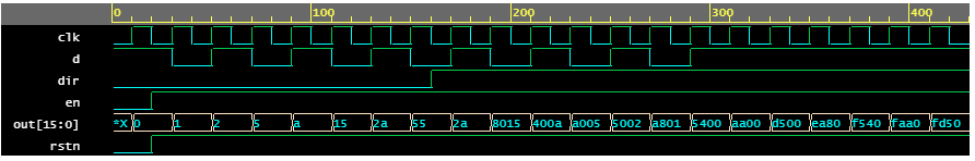
Hardware Schematic
Testbench
The testbench is used to verify the functionality of this shift register. The design is instantiated into the top module and the inputs are driven with different values. The design behavior for each of the inputs can be observed at the output pin out.
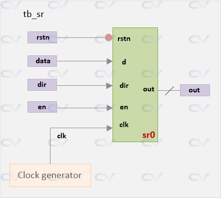
module tb_sr;
   parameter MSB = 16;        // [Optional] Declare a parameter to represent number of bits in shift register

   reg data;                  // Declare a variable to drive d-input of design
   reg clk;                   // Declare a variable to drive clock to the design
   reg en;                    // Declare a variable to drive enable to the design
   reg dir;                   // Declare a variable to drive direction of shift registe
   reg rstn;                  // Declare a variable to drive reset to the design
   wire [MSB-1:0] out;        // Declare a wire to capture output from the design

   // Instantiate design (16-bit shift register) by passing MSB and connect with TB signals
   shift_reg  #(MSB) sr0  (  .d (data),
                             .clk (clk),
                             .en (en),
                             .dir (dir),
                             .rstn (rstn),
                             .out (out));

   // Generate clock time period = 20ns, freq => 50MHz
   always #10 clk = ~clk;

   // Initialize variables to default values at time 0
   initial begin
      clk <= 0;
      en <= 0;
      dir <= 0;
      rstn <= 0;
      data <= 'h1;
   end

   // Drive main stimulus to the design to verify if this works
   initial begin

      // 1. Apply reset and deassert reset after some time
      rstn <= 0;
      #20 rstn <= 1;
          en <= 1;

	  // 2. For 7 clocks, drive alternate values to data pin
      repeat (7) @ (posedge clk)
         data <= ~data;

     // 4. Shift direction and drive alternate value to data pin for another 7 clocks
      #10 dir <= 1;
      repeat (7) @ (posedge clk)
         data <= ~data;

      // 5. Drive nothing for next 7 clocks, allow shift register to simply shift based on dir
      repeat (7) @ (posedge clk);

      // 6. Finish the simulation
      $finish;
   end

   // Monitor values of these variables and print them into the logfile for debug
   initial
      $monitor ("rstn=%0b data=%25b%2c.html en=%0b, dir=%0b, out=%b", rstn, data, en, dir, out);
endmodule
The time when shift register is enabled is highlighted in green in the log given below. The time when it shifts its direction is highlighted in yellow. The time when data input pin remains constant is highlighted in blue.
ncsim> run
rstn=0 data=1, en=0, dir=0, out=xxxxxxxxxxxxxxxx
rstn=0 data=1, en=0, dir=0, out=0000000000000000
rstn=1 data=1, en=1, dir=0, out=0000000000000000
rstn=1 data=0, en=1, dir=0, out=0000000000000001
rstn=1 data=1, en=1, dir=0, out=0000000000000010
rstn=1 data=0, en=1, dir=0, out=0000000000000101
rstn=1 data=1, en=1, dir=0, out=0000000000001010
rstn=1 data=0, en=1, dir=0, out=0000000000010101
rstn=1 data=1, en=1, dir=0, out=0000000000101010
rstn=1 data=0, en=1, dir=0, out=0000000001010101
rstn=1 data=0, en=1, dir=1, out=0000000001010101
rstn=1 data=1, en=1, dir=1, out=0000000000101010
rstn=1 data=0, en=1, dir=1, out=1000000000010101
rstn=1 data=1, en=1, dir=1, out=0100000000001010
rstn=1 data=0, en=1, dir=1, out=1010000000000101
rstn=1 data=1, en=1, dir=1, out=0101000000000010
rstn=1 data=0, en=1, dir=1, out=1010100000000001
rstn=1 data=1, en=1, dir=1, out=0101010000000000
rstn=1 data=1, en=1, dir=1, out=1010101000000000
rstn=1 data=1, en=1, dir=1, out=1101010100000000
rstn=1 data=1, en=1, dir=1, out=1110101010000000
rstn=1 data=1, en=1, dir=1, out=1111010101000000
rstn=1 data=1, en=1, dir=1, out=1111101010100000
rstn=1 data=1, en=1, dir=1, out=1111110101010000
Simulation complete via $finish(1) at time 430 NS + 0