Module ports and interfaces by default do not specify any timing requirements or synchronization schemes between signals. A clocking block defined between clocking and endcocking does exactly that. It is a collection of signals synchronous with a particular clock and helps to specify the timing requirements between the clock and the signals.
This would allow test writers to focus more on transactions rather than worry about when a signal will interact with respect to a clock. A testbench can have many clocking blocks, but only one block per clock.
Syntax
	[default] clocking [identifier_name] @ [event_or_identifier]
		default input #[delay_or_edge] output #[delay_or_edge]
		[list of signals]
	endclocking
Design
module pr_en ( input [7:0] a,
               input [7:0] b,
               input [7:0] c,
               input [7:0] d,
               input [1:0] sel,
               output reg [7:0] out);

   always @ (a or b or c or d or sel) begin
      if (sel == 2'b00)
         out <= a;
      else if (sel == 2'b01)
         out <= b;
      else if (sel == 2'b10)
         out <= c;
      else
         out <= d;
   end
endmodule
Hardware Schematic
Testbench
module tb_4to1_mux;
   reg [7:0] a;
   reg [7:0] b;
   reg [7:0] c;
   reg [7:0] d;
   wire [7:0] out;
   reg [1:0] sel;
   integer i;

   pr_en    pr_en0 (   .a (a),
                           .b (b),
                           .c (c),
                           .d (d),
                           .sel (sel),
                           .out (out));

   initial begin
      sel <= 0;
      a <= $random;
      b <= $random;
      c <= $random;
      d <= $random;

      for (i = 1; i < 4; i=i+1) begin
         #5 sel <= i;
      end

      #5 $finish;
   end
endmodule
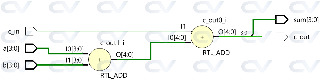
An adder is a digital component that performs addition of two numbers. Its the main component inside an ALU of a processor and is used to increment addresses, table indices, buffer pointers and in a lot of other places where addition is required.
A full adder adds a carry input along with other input binary numbers to produce a sum and a carry output.
Truth Table
| A | B | Cin | Cout | Sum |
|---|---|---|---|---|
| 0 | 0 | 0 | 0 | 0 |
| 0 | 0 | 1 | 0 | 1 |
| 0 | 1 | 0 | 0 | 1 |
| 0 | 1 | 1 | 1 | 0 |
| 1 | 0 | 0 | 0 | 1 |
| 1 | 0 | 1 | 1 | 0 |
| 1 | 1 | 0 | 1 | 0 |
| 1 | 1 | 1 | 1 | 1 |
Design
An example of a 4-bit adder is shown below which accepts two binary numbers through the signals a and b which are both 4-bits wide. Since an adder is a combinational circuit, it can be modeled in Verilog using a continuous assignment with assign or an always block with a sensitivity list that comprises of all inputs. The code shown below is that of the former approach.
module fulladd (  input [3:0] a,
                  input [3:0] b,
                  input c_in,
                  output c_out,
                  output [3:0] sum);

   assign {c_out, sum} = a + b + c_in;
endmodule
The code shown below uses an always block which gets executed whenever any of its inputs change value.
module fulladd (  input [3:0] a,
                  input [3:0] b,
                  input c_in,
                  output reg c_out,
                  output reg [3:0] sum);

	always @ (a or b or c_in) begin
  	{c_out, sum} = a + b + c_in;
  end
endmodule
Hardware Schematic
Testbench
module tb_fulladd;
	// 1. Declare testbench variables
   reg [3:0] a;
   reg [3:0] b;
   reg c_in;
   wire [3:0] sum;
   integer i;

	// 2. Instantiate the design and connect to testbench variables
   fulladd  fa0 ( .a (a),
                  .b (b),
                  .c_in (c_in),
                  .c_out (c_out),
                  .sum (sum));

	// 3. Provide stimulus to test the design
   initial begin
      a <= 0;
      b <= 0;
      c_in <= 0;

      $monitor ("a=0x%0h b=0x%0h c_in=0x%0h c_out=0x%0h sum=0x%0h", a, b, c_in, c_out, sum);

		// Use a for loop to apply random values to the input
      for (i = 0; i < 5; i = i+1) begin
         #10 a <= $random;
             b <= $random;
         		 c_in <= $random;
      end
   end
endmodule
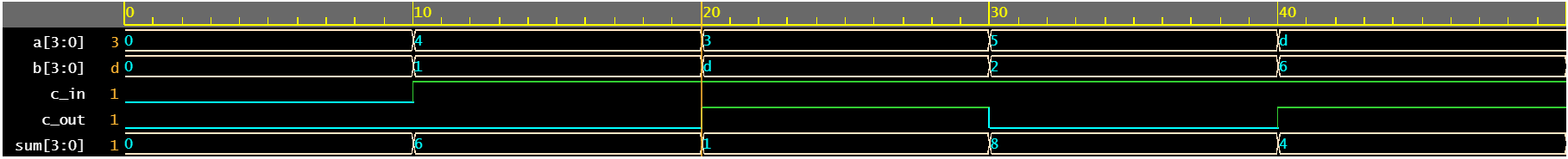
Note that when a and b add up to give a number more than 4 bits wide, the sum rolls over to zero and c_out becomes 1. For example, the line highlighted in yellow adds up to give 0x11 and the lower 4 bits get assigned to sum and bit#4 to c_out .
ncsim> run
a=0x0 b=0x0 c_in=0x0 c_out=0x0 sum=0x0
a=0x4 b=0x1 c_in=0x1 c_out=0x0 sum=0x6
a=0x3 b=0xd c_in=0x1 c_out=0x1 sum=0x1
a=0x5 b=0x2 c_in=0x1 c_out=0x0 sum=0x8
a=0xd b=0x6 c_in=0x1 c_out=0x1 sum=0x4
a=0xd b=0xc c_in=0x1 c_out=0x1 sum=0xa
ncsim: *W,RNQUIE: Simulation is complete.
What is a mux or multiplexer ?
A multiplexer or mux in short, is a digital element that transfers data from one of the N inputs to the output based on the select signal. The case shown below is when N equals 4. For example, a 4 bit multiplexer would have N inputs each of 4 bits where each input can be transferred to the output by the use of a select signal.
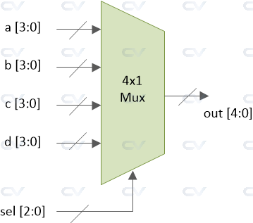
sel is a 2-bit input and can have four values. Each value on the select line will allow one of the inputs to be sent to output pin out.
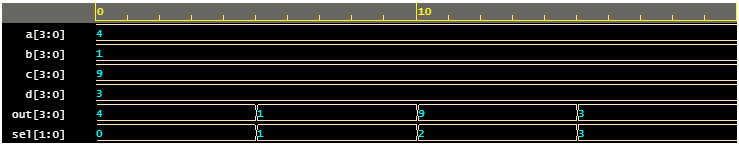
	sel     a     b     c     d     out
	 0     3    7     1     9    3
	 1      3    7    1     9    7
	 2      3     7    1    9    1
	 3      3     7     1    9   9
A 4x1 multiplexer can be implemented in multiple ways and here you'll see two of the most common ways:
- Using an
assignstatement - Using a
casestatement
Using assign statement
module mux_4to1_assign ( input [3:0] a,                 // 4-bit input called a
                         input [3:0] b,                 // 4-bit input called b
                         input [3:0] c,                 // 4-bit input called c
                         input [3:0] d,                 // 4-bit input called d
                         input [1:0] sel,               // input sel used to select between a,b,c,d
                         output [3:0] out);             // 4-bit output based on input sel

   // When sel[1] is 0, (sel[0]? b:a) is selected and when sel[1] is 1, (sel[0] ? d:c) is taken
   // When sel[0] is 0, a is sent to output, else b and when sel[0] is 0, c is sent to output, else d
   assign out = sel[1] ? (sel[0] ? d : c) : (sel[0] ? b : a);

endmodule
The module called mux_4x1_assign has four 4-bit data inputs, one 2-bit select input and one 4-bit data output. The multiplexer will select either a , b, c, or d based on the select signal sel using the assign statement.
Using case statement
Note that the signal out is declared as a reg type because it is used in a procedural block like always.
module mux_4to1_case ( input [3:0] a,                 // 4-bit input called a
                       input [3:0] b,                 // 4-bit input called b
                       input [3:0] c,                 // 4-bit input called c
                       input [3:0] d,                 // 4-bit input called d
                       input [1:0] sel,               // input sel used to select between a,b,c,d
                       output reg [3:0] out);         // 4-bit output based on input sel

   // This always block gets executed whenever a/b/c/d/sel changes value
   // When that happens, based on value in sel, output is assigned to either a/b/c/d
   always @ (a or b or c or d or sel) begin
      case (sel)
         2'b00 : out <= a;
         2'b01 : out <= b;
         2'b10 : out <= c;
         2'b11 : out <= d;
      endcase
   end
endmodule
The module called mux_4x1_case has four 4-bit data inputs, one 2-bit select input and one 4-bit data output. The multiplexer will select either a , b, c, or d based on the select signal sel using the case statement.
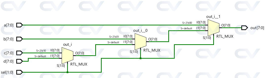
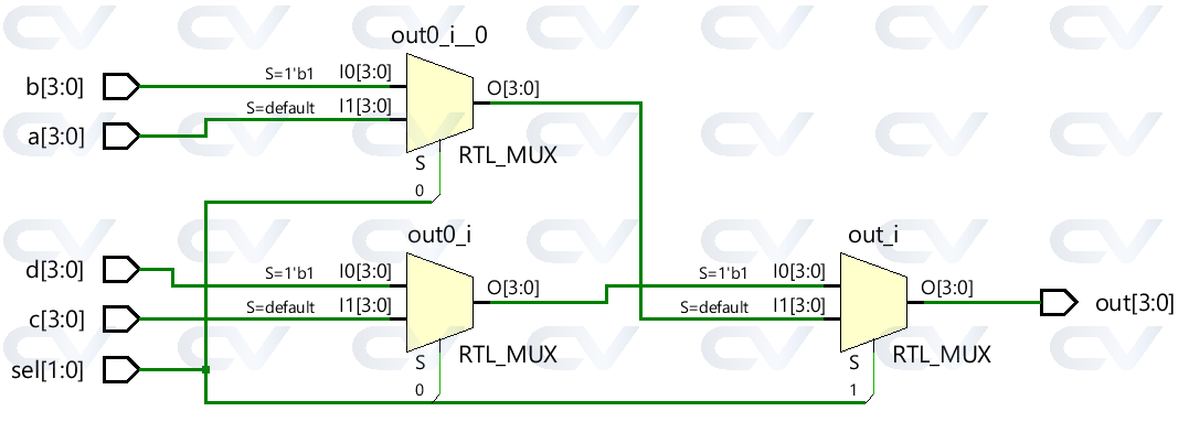
Hardware Schematic
Both types of multiplexer models get synthesized into the same hardware as shown in the image below.
Testbench
module tb_4to1_mux;

   // Declare internal reg variables to drive design inputs
   // Declare wire signals to collect design output
   // Declare other internal variables used in testbench
   reg [3:0] a;
   reg [3:0] b;
   reg [3:0] c;
   reg [3:0] d;
   wire [3:0] out;
   reg [1:0] sel;
   integer i;

   // Instantiate one of the designs, in this case, we have used the design with case statement
   // Connect testbench variables declared above with those in the design
   mux_4to1_case  mux0 (   .a (a),
                           .b (b),
                           .c (c),
                           .d (d),
                           .sel (sel),
                           .out (out));

   // This initial block is the stimulus
   initial begin
      // Launch a monitor in background to display values to log whenever a/b/c/d/sel/out changes
      $monitor ("[%0t] sel=0x%0h a=0x%0h b=0x%0h c=0x%0h d=0x%0h out=0x%0h", $time, sel, a, b, c, d, out);

   	  // 1. At time 0, drive random values to a/b/c/d and keep sel = 0
      sel <= 0;
      a <= $random;
      b <= $random;
      c <= $random;
      d <= $random;

      // 2. Change the value of sel after every 5ns
      for (i = 1; i < 4; i=i+1) begin
         #5 sel <= i;
      end

      // 3. After Step2 is over, wait for 5ns and finish simulation
      #5 $finish;
   end
endmodule
ncsim> run
[0] sel=0x0 a=0x4 b=0x1 c=0x9 d=0x3 out=0x4
[5] sel=0x1 a=0x4 b=0x1 c=0x9 d=0x3 out=0x1
[10] sel=0x2 a=0x4 b=0x1 c=0x9 d=0x3 out=0x9
[15] sel=0x3 a=0x4 b=0x1 c=0x9 d=0x3 out=0x3
Simulation complete via $finish(1) at time 20 NS + 0
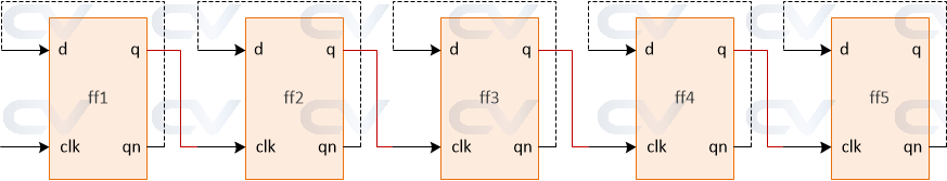
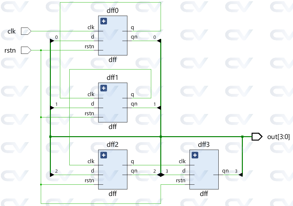
A ripple counter is an asynchronous counter in which the all the flops except the first are clocked by the output of the preceding flop.
Design
module dff (   input d,
               input clk,
               input rstn,
               output reg q,
               output qn);
   always @ (posedge clk or negedge rstn)
      if (!rstn)
         q <= 0;
      else
         q <= d;

   assign qn = ~q;
endmodule

module ripple ( input clk,
                input rstn,
                output [3:0] out);
   wire  q0;
   wire  qn0;
   wire  q1;
   wire  qn1;
   wire  q2;
   wire  qn2;
   wire  q3;
   wire  qn3;

   dff   dff0 ( .d (qn0),
                .clk (clk),
                .rstn (rstn),
                .q (q0),
                .qn (qn0));

   dff   dff1 ( .d (qn1),
                .clk (q0),
                .rstn (rstn),
                .q (q1),
                .qn (qn1));

   dff   dff2 ( .d (qn2),
                .clk (q1),
                .rstn (rstn),
                .q (q2),
                .qn (qn2));

   dff   dff3 ( .d (qn3),
                .clk (q2),
                .rstn (rstn),
                .q (q3),
                .qn (qn3));

   assign out = {qn3, qn2, qn1, qn0};

endmodule
Hardware Schematic
Testbench
module tb_ripple;
   reg clk;
   reg rstn;
   wire [3:0] out;

   ripple r0   (  .clk (clk),
                  .rstn (rstn),
                  .out (out));

   always #5 clk = ~clk;

   initial begin
      rstn <= 0;
      clk <= 0;

      repeat (4) @ (posedge clk);
      rstn <= 1;

      repeat (25) @ (posedge clk);
      $finish;
   end
endmodule
