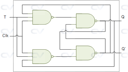
A T flip-flop can be implemented using NAND logic gates by performing the following steps:
- Use two NAND gates in a feedback loop where the output of one NAND gate connects to one of the inputs of the other NAND gate.
- Connect a T input to one of the inputs of each NAND gate.
- Connect an enable input to both NAND gates' inputs, with the enable signal flipped by an inverter to one of the inputs.
- Connect a clock input inverted to either one of the two inputs of each NAND gate.
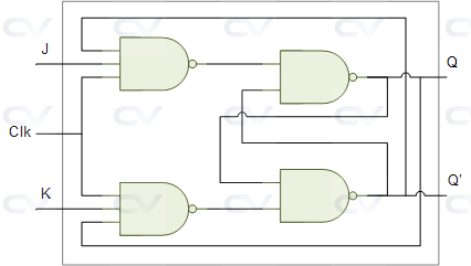
A JK flip-flop can also be implemented using NAND logic gates by performing the following steps:
- Use two NAND gates in a feedback loop where the output of one NAND gate connects to one of the inputs of the other NAND gate.
- Connect a J and a K input to the inputs of the two NAND gates, respectively.
- Connect an enable input to both NAND gates' inputs, with the enable signal flipped by an inverter to one of the inputs.
- Connect a clock input inverted to either one of the two inputs of each NAND gate.
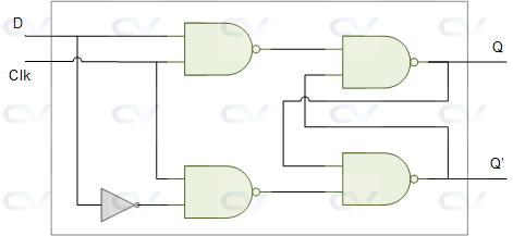
A D flip-flop can be implemented using NAND logic gates by performing the following steps:
- Connect two NAND gates in a cross-coupled arrangement, with the output of each gate connected to the input of the other gate.
- Connect the D input to one of the NAND gates' inputs.
- Connect a clock input to both NAND gates' inputs, with the clock signal flipped by an inverter to one of the inputs.
- Connect an enable input to both NAND gates' inputs, with the enable signal flipped by an inverter to one of the inputs.
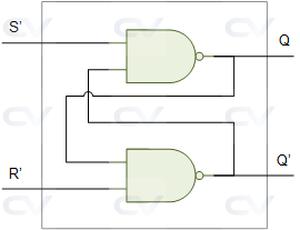
An SR latch can be implemented using NAND logic gates by performing the following steps:
- 1. Connect two NAND gates in a cross-coupled arrangement, with the output of each gate connected to the input of the other gate.
- 2. Connect SR inputs to the two NAND gates, where S is connected to one NAND gate's input and R is connected to the other NAND gate's input.
- 3. Connect the output of the NAND gate with S input to the input of the NAND gate with R input.
- 4. Connect the output of the NAND gate with R input to the input of the NAND gate with S input.
A sequential logic circuit is a type of digital circuit that can store and remember information or data between clock cycles. It uses a memory element, such as a flip-flop or register, to store and update the state of the circuit based on the input and previous state. These circuits can perform a variety of functions, such as counting, shifting, and detecting and responding to specific input patterns. Sequential logic circuits are commonly used in digital electronics, including computers, control systems, and communication devices.
